
")


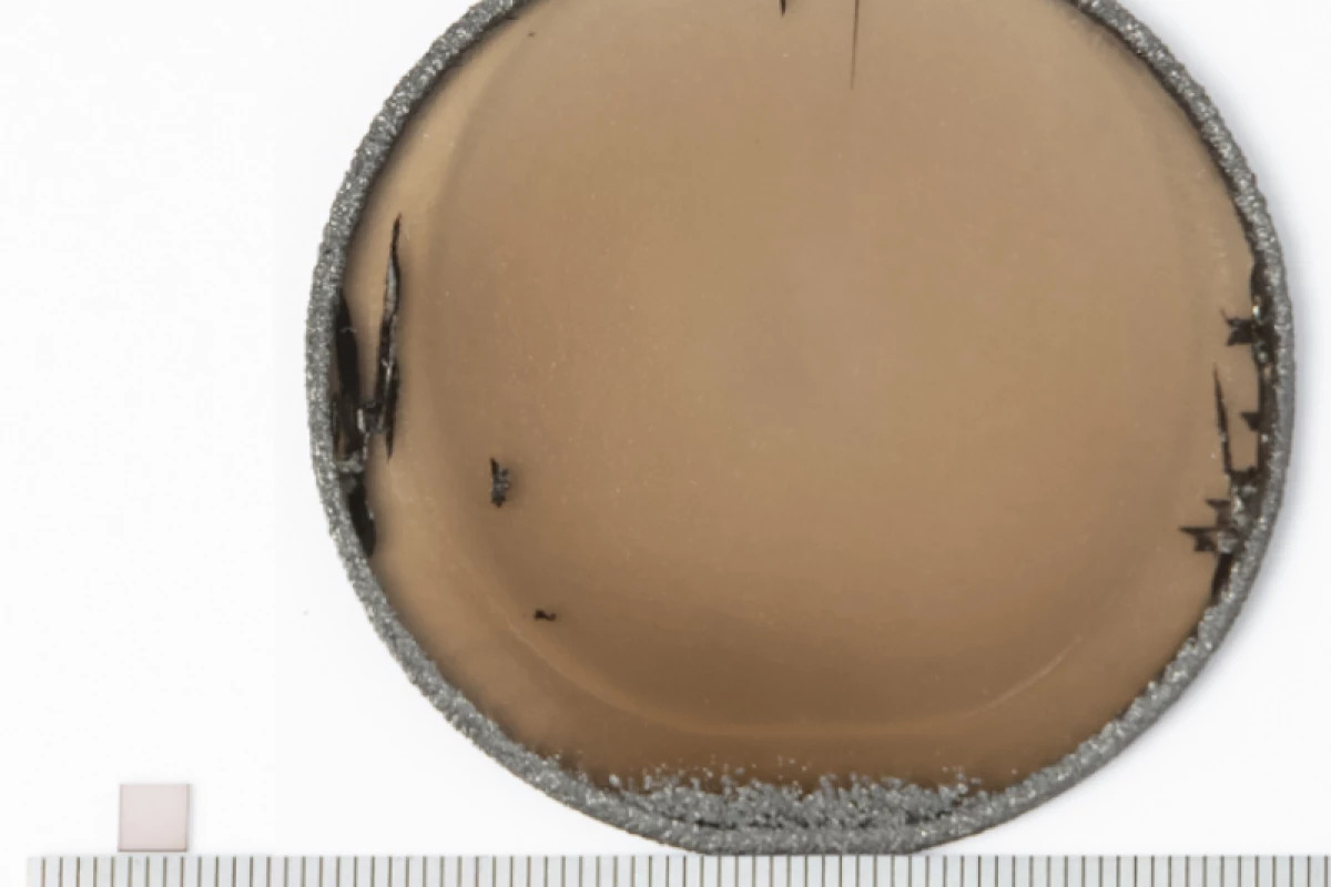
An ultra-pure diamond wafer (right) measuring 5 cm (2 in) in diameter that could be used for high-density data storage. The small square to the left is the usual size of diamond wafers possible using older manufacturing techniques. Saga University
–
Diamond is one of the most promising materials for practical quantum computing systems, including memory. A particular defect in the crystal, known as a nitrogen-vacancy center, can be used to store data in the form of superconducting quantum bits (qubits), but too much nitrogen in the diamond disrupts its quantum storage capabilities.
That meant there was a trade-off to make – scientists had to create either large diamond wafers with too much nitrogen, or ultra-pure diamond wafers that are too small to be of much use for data storage. But now, researchers at Saga University and Adamant Namiki Precision Jewelery Co. in Japan have developed a new method for manufacturing ultra-high purity diamond wafers that are big enough for practical use.
With this technique, the team says the resulting diamond wafers measure 5 cm across, and have such immense data density that they can theoretically store the equivalent of a billion Blu-Ray discs. One Blu-Ray can store up to 25 GB (assuming it’s single-layered), which would mean this diamond wafer should be able to store a whopping 25 exabytes (EB) of data. The company calls these wafers Kenzan Diamond.
The key is that these diamonds have a nitrogen concentration of under three parts per billion (ppb), making them incredibly pure. The researchers say that these are the largest wafers with that level of purity – most others only get to 4 mm2 (0.006 in2) at most.
Achieving this requires a new manufacturing technique. Diamond wafers are made by growing the crystals on a substrate material, and that material is usually a flat surface. The problem is, the diamond can crack under the strain, degrading the quality. In the new process, the team made a relatively simple change – the substrate surface was shaped like steps, which spreads the strain horizontally and prevents cracking. This allows them to make larger diamond wafers with higher purity.
The team hopes to commercialize these diamond wafers in 2023, and in the meantime are already working towards doubling the diameter to 10 cm (4 in).
The research will be presented at the International Conference on Compound Semiconductor Manufacturing Technology in May.
Sources: Saga University, Adamant Namiki
–
–
Most Viewed


–